
我是山东师范大学的一名模拟IC设计方向的研二学生,指导老师是华庆(Qing Hua)。研一时跟随导师的指导,做高压驱动芯片设计(1um),熟悉设计软件和设计流程。同时自学拉扎维和桑森的书籍,沉淀模拟电路设计的基本功底。研二,开始由高压驱动芯片电路里的模块引申,例如电平位移和电压基准源电路,进行小模块电路创新设计。通过对相关方向论文的研究和总结,不断尝试,自主设计了带浮动衬底的电平位移电路(130nm)和带差分式输出的电压基准源电路(180nm),另外还设计了三支路逻辑控制的电平位移电路(55nm),有望发表三篇质量中上的论文。有读博继续深造的打算,要做就做最好。目前对IC电源方向(亚阈值低功耗)这一块积累较为深刻,对其它模拟IC方向抱有期待。
📖 教育背景
-
2019.09 - 2023.06, 土木工程, 成都大学(软科232).
大二决心学IC设计,自学电路基础、模拟电子技术基础、数字电子技术基础、信号与系统、半导体物理等多门课程
-
2023.09 - 至今, 电子科学与技术, 山东师范大学(软科105).
自学《模拟CMOS集成电路设计》、《模拟集成电路设计精粹》等书籍
🔥 模拟IC设计经历
-
2023.10~2024.6 :600V高压驱动芯片-1um
1、参与七通道驱动芯片设计:包括欠压保护电路,电平位移电路,高边驱动脉冲信号产生电路等。
2、两通道驱动芯片:每个模块的电路设计和版图设计。电路能将5V的输入信号驱动600V高边输出和15V低边输出。最终半桥式驱动功率器件。对电压基准和电平位移等部分进行优化,达到了低延时的电路特性。
-
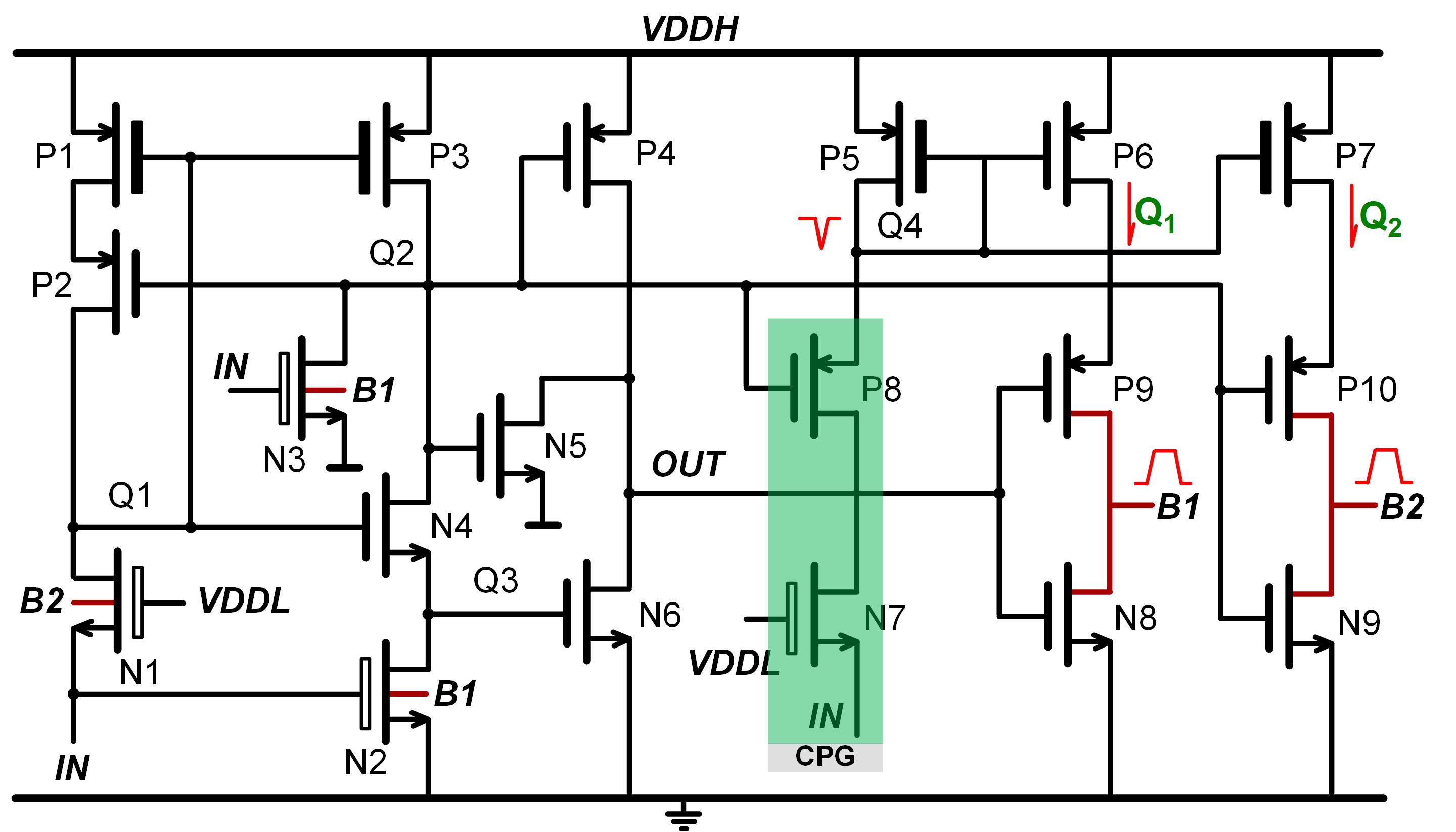
2024.04~2024.8:带浮动衬底的电平位移电路-130nm
1、提出了一种浮动衬底技术,根据电路输出逻辑,反馈提供延时的大小可控的浮动电压,给电路输入直接驱动的正反逻辑器件提供衬底偏置。周期性地降低器件的阈值电压,同时降低电平位移时上下沿的延迟时间,小于2nS,最小输入电压降至0.17V。
2、提出了一种电平位移基础结构,带有动态电流限制器件,同时降低了开关状态的静态功耗。最终EDP优于同类型平均水平一个数量级
-
2024.08~2024.12:三支路逻辑控制电平位移-55nm
1、设计了三支路逻辑控制的电平位移,具有非常低的静态功耗,比同制程电路有更快的转换速度。
-
2024.04~2024.12:CMOS电压基准源设计-180nm
1、提出了上厚下薄的伪共源共栅电流镜。提供的偏置电流精度非常高,输出电流偏差占比小于0.02%
2、提出了两级自偏置的SDMT核心。提供两个参考电压。电压自偏置降低LS。
3、提出了串联差分式输出结构。将两个参考电压进行差分,抵消PVT带来的偏差,并给予PVT补偿。通过差分和补偿,LS降低一半,PSRR全频域至少下降6dB,工艺角偏差小于10mV。温度偏差下降至1mV以内。
4、提出关键极点偏移技术。PSRR极值下降了20%。通过极点叠加加速PSRR衰减,高频PSRR下降了7dB。
5、提出了双输入启动电路。与单输入启动电路相比,静态功耗下降了三个数量级。
📝 成果转换
«A Floating Bias Technique Enabled Voltage Level Shifter Operating in Subthreshold Voltage Input with Ultra-Low Symmetric Delay»
Qun Zhou, Kang Zeng, Weiwei Yue and Qing Hua, Member, IEEE
IEEE Transactions on Circuits and Systems II: Express Briefs (TCAS-II)
未流片
Abstract
This brief presents an ultra-fast voltage level shifter (VLS) with a wide voltage conversion range. The proposed VLS achieves low symmetric propagation delay while operating in the subthreshold voltage, utilizing a newly introduced floating bias technique (FBT). By integrating a novel dynamic current limiter structure with a split inverter and pull-down devices, both the low-to-high and high-to-low delays are largely reduced. The design of the proposed VLS is divided into two sections: the basic version and the enhanced version, which incorporates the FBT. Using a standard 130nm CMOS technology, the basic version demonstrates low propagation delay and high energy efficiency. Post-layout simulations, taking into account process, voltage, and temperature (PVT) variations, have been performed. With the implementation of the FBT, the delay is reduced to 2.09ns, dynamic power consumption is lowered to 27.3fJ, the minimum supply voltage is 0.17V, and the static power consumption is 9.7nW for the enhanced version.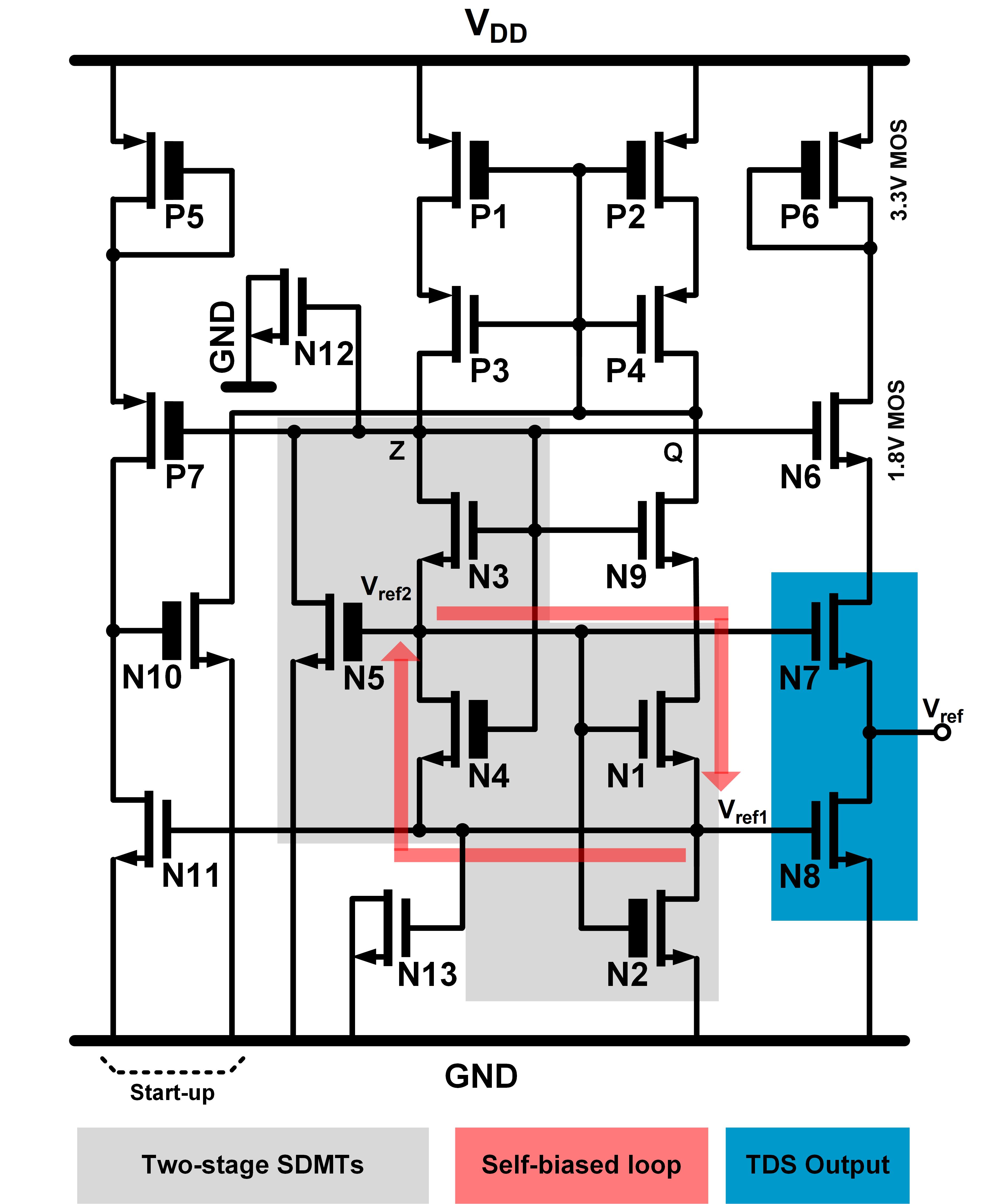
«A two-stage self-bias SDMTs CMOS voltage reference achieving active optimization with PVT variation by tandem differential structure»
Qun Zhou, Yaoze Liu, Kang Zeng, Changchun Zhou and Qing Hua,Member, IEEE
IEEE Transactions on Circuits and Systems–I: Regular Papers (TCAS-I)
完成流片
Abstract
It's waited to be finished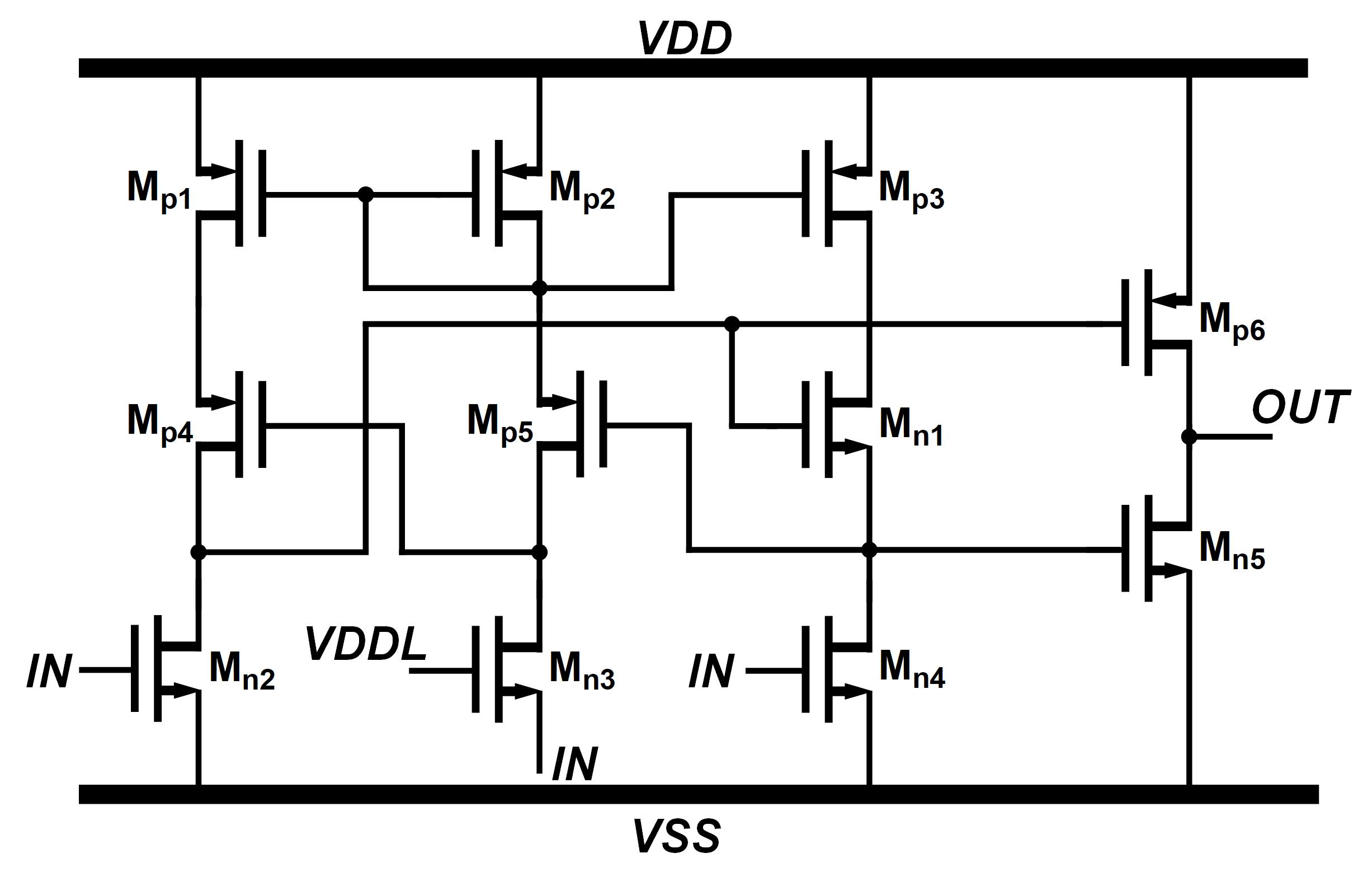
55nm的三支路逻辑控制的电平位移
完成流片
Abstract
It's waited to be finished🍀 流片经历
«A two-stage self-bias SDMTs CMOS voltage reference achieving active optimization with PVT variation by tandem differential structure»
12/2024, Project Leader (designed and testing)
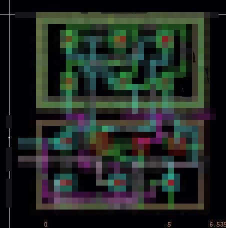
Fabricated in SMIC 180-nm technology with an area of 185 um×26 um
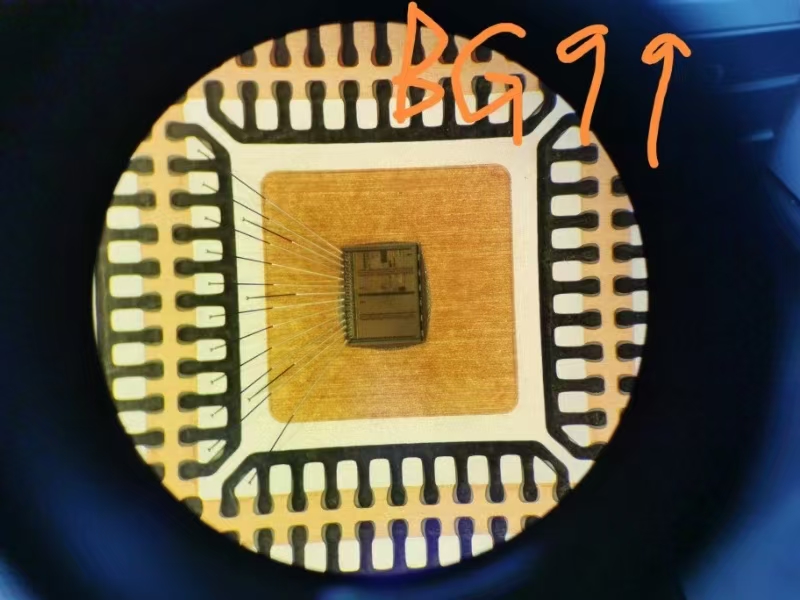
三支路逻辑控制的电平位移电路
06/2025 (Expected), Collaboration(designed and testing)
Fabricated in SMIC 55-nm technology with an expected area of 6 um×8 um
💬 个人自评
有目标有规划,自驱力强,抗压能力强,能有效解决研究过程中碰到的问题。英语口语能力不错,能和外国人无障碍交流。学习能力强,硕士阶段很多研究方向都是由自己挖掘。希望能在未来博导的指引和教导下,在博士期间,至少发表一篇顶刊。如果有博导感兴趣,可以收藏我的简历CV